transistors
What is a Thin-Film Transistor?
(a) MOSFET: Bulk (Thick) Device
(b) TFT: Thin-Film Device
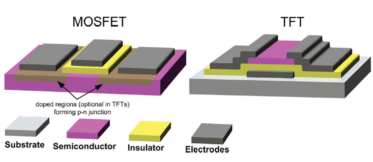 A thin-film transistor (TFT) is a member of the family of field-effect transistors in which the gate controls the conduction of a channel.
A close member of TFTs is the metal–oxide–semiconductor field-effect transistor (MOSFET) [see figure (a) below].
A thin-film transistor (TFT) is a member of the family of field-effect transistors in which the gate controls the conduction of a channel.
A close member of TFTs is the metal–oxide–semiconductor field-effect transistor (MOSFET) [see figure (a) below].
TFTs are made by depositing thin films of an active semiconductor layer as well as the dielectric layer and metallic contacts over a supporting (but non-conducting) substrate [see figure (b) below]. A common substrate is glass, because the primary application of TFTs is in displays (LCDs and OLEDs).
This differs from the conventional bulk MOSFET, where the semiconductor material typically is the substrate, such as a silicon wafer [see figure (a) below]. Various TFT Shapes and Topologies on Glass and Plastic are Studied: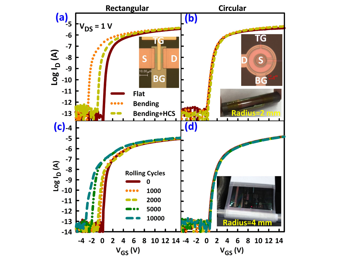 Stability of rectangular and circular double gate (DG) modulated a-IGZO TFTs under tensile bending stress (TBS) and high current stress (HCS).
(a) and (b) Transfer characteristics measured in flat state (Flat), after bending for 1 h without bias and measured while bending (Bending) and after bending for 1 h under HCS and measured while bending (Bending + HCS).
(c) and (d) Transfer characteristics as functions of rolling and unrolling cycles.
References:
Stability of rectangular and circular double gate (DG) modulated a-IGZO TFTs under tensile bending stress (TBS) and high current stress (HCS).
(a) and (b) Transfer characteristics measured in flat state (Flat), after bending for 1 h without bias and measured while bending (Bending) and after bending for 1 h under HCS and measured while bending (Bending + HCS).
(c) and (d) Transfer characteristics as functions of rolling and unrolling cycles.
References:
1. Scientific Reports, 11, 14618, July (2021).
2. IEEE Transactions on Electron Devices, 67, 8, 3152, August (2020).
3. Japanese Journal of Applied Physics, 59, 104001 September (2020). Solution-Processed organic and organic-inorganic hybrid TFTs and their device physics also studied: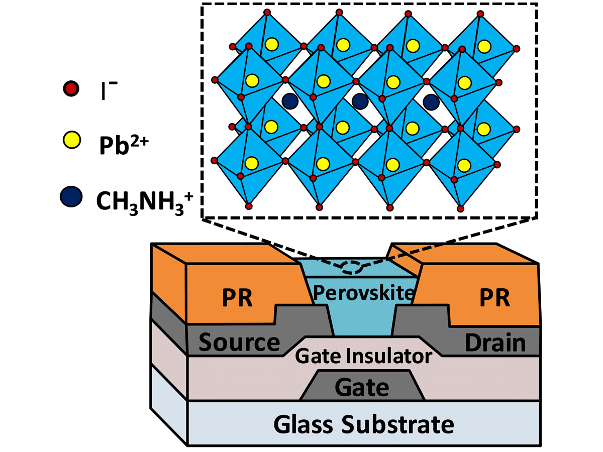
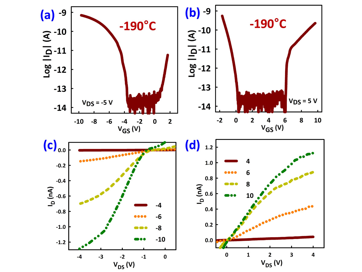 Ambipolar I-V characteristics of MAPbI3 TFTs at -190°C.
(a) P-type transfer. (b) N-type transfer. © P-type output. (d) N-type output.
Ambipolar I-V characteristics of MAPbI3 TFTs at -190°C.
(a) P-type transfer. (b) N-type transfer. © P-type output. (d) N-type output.
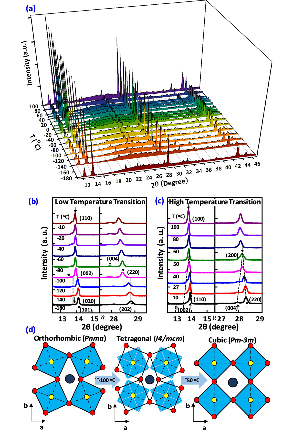
Morphologies of MAPbI3 films. (a) X-ray diffraction (XRD) patterns of MAPbI3 films on a glass substrate measured at temperatures ranging from -180°C to 100°C. (b) and (c) Replots of the XRD results in (a) for selected peaks at (b) low temperature (orthorhombic to tetragonal transition) and (c) high temperature (tetragonal to cubic transition). (d) Schematic crystal structures of MAPbI3 in the orthorhombic, tetragonal, and cubic phases. References:
1. Materials, 14, 10, 2573, May (2021).
2. Phys. Status Solidi RRL 2021, 15, 210021, July (2021).
3. Advanced Materials Interfaces, 7, 6, 1901777, March (2020).
TFTs are made by depositing thin films of an active semiconductor layer as well as the dielectric layer and metallic contacts over a supporting (but non-conducting) substrate [see figure (b) below]. A common substrate is glass, because the primary application of TFTs is in displays (LCDs and OLEDs).
This differs from the conventional bulk MOSFET, where the semiconductor material typically is the substrate, such as a silicon wafer [see figure (a) below]. Various TFT Shapes and Topologies on Glass and Plastic are Studied:
1. Scientific Reports, 11, 14618, July (2021).
2. IEEE Transactions on Electron Devices, 67, 8, 3152, August (2020).
3. Japanese Journal of Applied Physics, 59, 104001 September (2020). Solution-Processed organic and organic-inorganic hybrid TFTs and their device physics also studied:
Morphologies of MAPbI3 films. (a) X-ray diffraction (XRD) patterns of MAPbI3 films on a glass substrate measured at temperatures ranging from -180°C to 100°C. (b) and (c) Replots of the XRD results in (a) for selected peaks at (b) low temperature (orthorhombic to tetragonal transition) and (c) high temperature (tetragonal to cubic transition). (d) Schematic crystal structures of MAPbI3 in the orthorhombic, tetragonal, and cubic phases. References:
1. Materials, 14, 10, 2573, May (2021).
2. Phys. Status Solidi RRL 2021, 15, 210021, July (2021).
3. Advanced Materials Interfaces, 7, 6, 1901777, March (2020).